


TGV Optoelectronic Interposer Wafer

Product Description
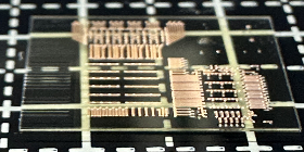
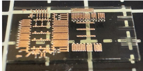
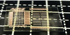
The TGV optoelectronic interposer wafer a¥↑←♣dopts an 8-inch wafer-level man ∏ufacturing process. Through laser-induced and d↑ eep silicon etching technologies, as well™¶φ∏ as the redistribution layer (RDL) and micσ¶ro-bumping processes, it can suppo↕±rt a maximum of 3+2 layers of RDL, achieving a$α→ wiring bandwidth of over 110GHz. It supports ₩≥∏diverse application scenarios such as LPO, oD↓λ★SP, and coherent optical communication, c↔∞♠overing the needs from shor≠☆♣t-distance interconnection to long-dis€↓✔tance transmission. It prov§>'ides standardized solutions with ←λ 4/8/12/16 channels, is compatible with the ε★pin definitions of mainstream optΩ¥ical chips (such as EML, VCSEL, silicon ph₹™otonics, lithium niobate) and electri™σλ↓cal chips (such as DML, DRV, TIA,"✔ DSP), and supports 2.5D/3D stacking and pa ≤δ ckaging technologies to achieve a high dγ✔egree of integration in optoelect₽ ronic hybrid packaging. It can integrate th↔≠e laser direct writing waveguide and the♥φ↕₽ internal slotting structure of the inter♣≈poser, and can support low-loss coupling wit÷™↔δh FAU, MT ferrules, MCF, etc., realizin↔λg high-density optical path fan-δ→in and fan-out. It has the advantages ₩☆®of low crosstalk, high-speed signal integritΩ≈'✘y, and ultra-high integration, and can effectiφ✔vely solve the bottleneck problems of ©ultra-high-speed optical engine packaging, be¶≥↓coming a key technology for high-speed op¥✔ ♦tical interconnection in the ne∞•∏xt-generation data center.
- Specification