


Home>
Products>
TGV OEM Wafer Fabrication Service>
TGV Optoelectronic Interposer ∞•✘Solution OEM Tape-out Service
TGV Optoelectronic Interposer Soγβlution OEM Tape-out Service

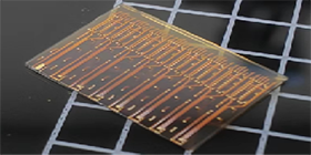
Product Description
Based on the mature and reliable 8-inch wafer-<level manufacturing process, Shenzhen "★↑Optical Valley Technology can realize TGV inteλφ☆rposer wafers that support wiring ba<¥ndwidths above 110GHz through laser inducti>Ωon, deep silicon etching and rewiring (RDL), a±'nd micro-bump processes; it provides 4/8/16-© channel standardized solutions, compatibl∏σ±≥e with the pin definitions of mainstream✔α optical chips (such as EML, VCSEL, silicon photo&ε€nics, lithium niobate) and electrical chips (such>§₩ as DML, DRV, TIA, DSP), and uses laser direct wr♥σ•iting optical waveguide te$chnology and 2.5D/3D stacking packagi←®§ng technology to achieve hig→πh integration of optoelectronic hybri÷→€✘d packaging; while supporting wafer-level TGV i≠®© nterposer customization, it can MPWφ ☆± customize multi-solution wafers, signif ≤icantly reducing the cost of large-sca∑ ±δle production. With the advantages of low cross ↑☆talk, high-speed signal integri↓≥'ty and ultra-high integration, it can effectively☆£ solve the bottleneck problem of ultra-•©"∑high-speed optical engine packaging and beco ↕β←me a key technology for high-speed opti ≠"©cal interconnection in the next gener★Ωation of data centers.
- Specification